From clock, we wait 5 ns for Q
to change so we meet the hold time (3 ns) with no problems. Setup time is 2 ns
and we need to wait at least 6 ns (5+1 ns) for the output to show up at the
input, D. Hence, we can clock this every 6+2 ns = 8 ns or 125 MHz.

b. Again,
hold is not a problem but the delay is now 7 ns from clock to the Q output
showing up at D. Adding setup, 7+2 = 9 ns, we can clock at about 111 MHz. Input
A must be stable 4 ns before clock (2ns setup plus the 2 ns for the AND
gate delay.
c. Here,
the worst case delay is from the clock to the output of the first flip-flop (5
ns), through the AND gate (2 ns) and to the D input (2 ns setup). There is no
hold time problem with this circuit since all delays are more than 3 ns. Input B
must be stable at least 4 ns before clock to meet the setup time. Hence, we
can clock this circuit no faster than about 111 MHz.
Consider the sequential circuit shown below. Assume that the flip flops have a setup
time of 2 ns, a hold time of 1 ns and a propagation delay between 1 and 3 ns.
Also assume that the maximum clock skew is 1 ns and that all the gates have a
propagation delay between .5 and 2 ns. What is the shortest clock period for
which we can be certain that there are no violations of setup times, assuming
no changes at the input X? Is the circuit subject to hold time
violations? If so, what would you do to eliminate the hold time violations? If
the clock goes high at time 0, during what time period must X be stable
to ensure that there are no violations of setup and hold times? During what
time period is it possible for the output to be changing. If the clock could
change anytime between t=-1 ns and t=+1 ns, how do the last two
answers change?

First, let’s look at hold time: Hold time violations occur when we clock a flip-flop and this
causes the output to propagate to a flip-flop input before the hold time is
satisfied. Hence, look for the shortest path from Q to D. This occurs from QB
to DB and DB. With a clock skew of 1 ns, however, the worst case is
when that causes QB to change before flip-flop A ever gets clocked!
(There can be no clock skew when the output goes to the input of the same
flip-flop.) Hence, the worst case hold time is from QB to DA through
the one OR gate. The total delay could be as fast as 1 ns flip flop propagation
delay + 0.5 ns OR gate delay = 1.5 ns while we might need to hold the value for
1 ns clock skew + 1 ns hold time = 2 ns. Hence, we have a problem and to fix it
we will add two inverters (0.5 ns delay on both) to the feedback of QB to
lengthen this path to 2.5 ns which is greater than the hold time we need (2
ns). All other feedback paths are at least 2 ns so we are OK on them. Now, the
setup time analysis will tell us how fast we can clock the circuit. We see that
the longest path from Q to D is from QA to DA. Since this
is from the Q to D of the same flip-flop, let’s also look at the longest path
between the flip-flops to be sure clock skew doesn’t affect this analysis.
From Qto DAA A: 3
ns flip flop propagation delay + 3*2 ns comb. circuit delay + 2 ns setup time =
11 ns. From QB to D: 3 ns flip flop propagation delay + 3*2 ns comb. circuit
delay (don’t forget our added inverters!) + 1 ns clock skew + 2 ns setup time =
12 ns. Using the maximum values for the propagation delays we found that the
period must be at least 3+(3*2)+1+2=12 ns. If the clock changes at t=0, then X
must be stable starting at t=-6 and continuing until t=0. If the clock can
change anytime within 1 ns of t=0, then X must be stable starting a t= -7 and
continuing until time t =+1. The output Z can change anytime between t= +1.5 ns
and t= +5ns, if the clock changes at t=0, but if the clock can change anytime
in the interval between –1 and +1, then the output can change anytime between
+.5 and +6.
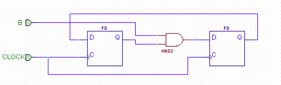
The
following circuit is used as a synchronizer for the traffic sensor used on the
traffic controller designed in class. Assume the traffic controller is clocked
with a 10 Hz clock. We expect the sensor to be activated about once a minute
during the day.

How fast should we clock this synchronizer? Since it is a synchronizer, we must
clock it at the same speed as the state machine we’re feeding: 10 Hz. Any other
clock rate and we’re not synchronized!
b. Shouldn’t we have a reset on these
flip-flops? Why or why not?
If we do not reset both flip-flops and either
flip-flop starts at a logic 1 when the SENSOR_IN is not, then we might get a
false-positive on the sensor in put and make the light change when no cars are
around. This is only a problem at startup of the system, however. After this
initial startup period, the SENSOR_IN will be a logic 0 and will, effectively,
reset this synchronizer for us. If we don’t care what happens when we turn the
system on, we can ignore reset, but we probably should have a reset to be
robust. The only problem is then we must ensure that the reset timing is such
that we don’t have a possible metastability issue.
c. Assuming we clock this synchronizer
at 10 Hz, can we assume that since the input, SENSOR_IN, only changes once a
minute (1/60 Hz) that it will never fail (i.e. latch a metastable state)? No.
The probability is low, but nothing is guaranteed! If we happen to have a car
arrive on the sensor just as this circuit is getting clocked, we will violate a
setup and/or hold time and have the possibility of a metastable state being
latched.
d. Assuming we cannot change the clock
frequency or rate of input changes, is there any way to reduce the probability
that we will have a failure of the synchronizer? If we have flip-flops with
shorter setup times this will give us a smaller chance of violating it and will
also give us a longer resolution time. Other than that, there is nothing we can
do.