Clock Domain Crossing. . .
The following section explains clock domain interfacing
One of the biggest challenges of system-on-chip (SOC) designs is that different blocks operate on independent clocks. Integrating these blocks
via the processor bus, memory ports, peripheral busses, and other interfaces can be troublesome because unpredictable behavior can result when the
asynchronous interfaces are not properly synchronized
A very common and robust method for synchronizing multiple data signals is a handshake technique as shown in diagram below This is popular
because the handshake technique can easily manage changes in clock frequencies, while minimizing latency at the crossing. However, handshake logic is
significantly more complex than standard synchronization structures.

FSM1(Transmitter) asserts the req (request) signal, asking the receiver to accept the data on the data bus.
FSM2(Receiver) generally a slow module asserts the ack (acknowledge) signal, signifying that it has accepted the data.
it has loop holes: when system Receiver samples the systems Transmitter req line and Transmitter samples system Receiver ack line, they have done it
with respect to their internal clock, so there will be setup and hold time violation. To avoid this we go for double or triple stage synchronizers,
which increase the MTBF and thus are immune to metastability to a good extent. The figure below shows how this is done.

Blocking vs Non-Blocking. . .
self triggering blocks -
module osc2 (clk);
output clk;
reg clk;
initial #10 clk = 0;
always @(clk) #10 clk <= ~clk;
endmodule
After the first @(clk) trigger, the RHS expression of the nonblocking assignment is
evaluated and the LHS value scheduled into the nonblocking assign updates event queue.
Before the nonblocking assign updates event queue is "activated," the @(clk) trigger
statement is encountered and the always block again becomes sensitive to changes on the
clk signal. When the nonblocking LHS value is updated later in the same time step, the
@(clk) is again triggered.
module osc1 (clk);
output clk;
reg clk;
initial #10 clk = 0;
always @(clk) #10 clk = ~clk;
endmodule
Blocking assignments evaluate their RHS expression and update their LHS value without
interruption. The blocking assignment must complete before the @(clk) edge-trigger
event can be scheduled. By the time the trigger event has been scheduled, the blocking
clk assignment has completed; therefore, there is no trigger event from within the always
block to trigger the @(clk) trigger.
Bad modeling: - (using blocking for seq. logic)
always @(posedge clk) begin
q1 = d;
q2 = q1;
q3 = q2;
end
Race Condition
always @(posedge clk) q1=d;
always @(posedge clk) q2=q1;
always @(posedge clk) q3=q2;
always @(posedge clk) q2=q1;
always @(posedge clk) q3=q2;
always @(posedge clk) q1=d;
always @(posedge clk) begin
q3 = q2;
q2 = q1;
q1 = d;
end
Bad style but still works

Good modeling: -
always @(posedge clk) begin
q1 <= d;
q2 <= q1;
q3 <= q2;
end
always @(posedge clk) begin
q3 <= q2;
q2 <= q1;
q1 <= d;
end
No matter of sequence for Nonblocking
always @(posedge clk) q1<=d;
always @(posedge clk) q2<=q1;
always @(posedge clk) q3<=q2;
always @(posedge clk) q2<=q1;
always @(posedge clk) q3<=q2;
always @(posedge clk) q1<=d;
Good Combinational logic :- (Blocking)
always @(a or b or c or d) begin
tmp1 = a & b;
tmp2 = c & d;
y = tmp1 | tmp2;
end
Bad Combinational logic :- (Nonblocking)
always @(a or b or c or d) begin will simulate incorrectly…
tmp1 <= a & b; need tmp1, tmp2 insensitivity
tmp2 <= c & d;
y <= tmp1 | tmp2;
end
Mixed design: -
Use Nonblocking assignment.
In case on multiple non-blocking assignments last one will win.
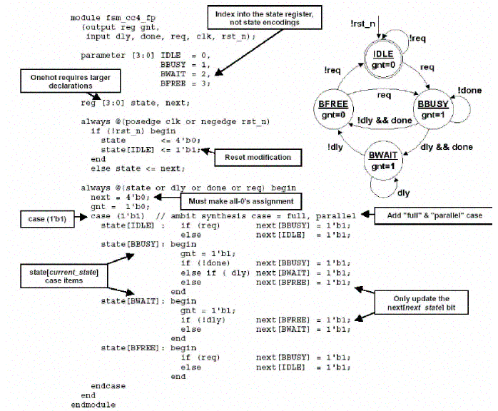
Verilog FSM


