
From the Cadence Verilog-A Language Reference Manual: "The Verilog-A language is a high-level language that uses modules to describe the structure and behavior of analog systems and their components. With the analog statements of Verilog-A, you can describe a wide range of conservative systems and signal-flow systems, such as electrical, mechanical, fluid dynamic, and thermodynamic systems."
This tutorial describes how to create Verilog-A code for an analog to digital converter (ADC) using the Modelwriter wizard. The tutorial also steps through the simulation of the symbol created from the Verilog-A code of the ADC. At the end of the tutorial, there are instructions on writing Verilog-A code for an inverter.
To begin with, let's build an analog to digital converter. We'll do this by using a wizard called Modelwriter. The wizard allows you to select from a group of devices and then choose the parameters for that device. Then, Modelwriter will create verilog-a code based on the characteristics of the device that you set.
First, start the Cadence tools by typing "icfb &" from your cadence directory in a shell window. In the Library Manager window, after highlighting your library, select File -> New -> Cell View ... Enter "adc" or something similar in the "Cell Name" field. In the "Cell View" field, enter "veriloga". That tool should automatically change to the Verilog-A Editor.
After selecting OK, the Invoke Modelwriter window will appear. Select OK.

Then, the Cadence Modelwriter window will appear and you can select a variety of components. Feel free to see what is available. For this tutorial, select the "Analog to Digital Converter" device in the "Interface" folder. Then, select Next>.

The next window includes all of the parameters of the analog to digital converter. Change the "Number of Bits" to 4 and the "Max. Input Voltage" and the "Min. Input Voltage" to 5 V and 0 V, respectively. Leave everything else as is. Select Next>.

The window below contains the verilog-a code generated by the wizard. Scroll through the code and try to understand the functions used. Select Save Generated Code at the bottom right corner of the screen. Then, select Finished! Exit in the same place.

You will be prompted about creating a symbol. Select Yes.

The Symbol Generation Options window will appear. All of the default settings should be fine. Therefore, go ahead and select OK.

The symbol for the ADC will appear in the Virtuoso Symbol Editing window. Make any changes desired to the shape to the symbol shape. Move "[@instanceName]" so that it is above the symbol and change the name of "[@partName]" to something like "ADC". After all changes have been made, select Design -> Check and Save or select F8 and then close the Virtuoso Symbol Editing window.

In order to simulate the ADC, a schematic view needs to be created. In the Library Manager window, after highlighting your folder, select File -> New -> Cell View. Name the Cell "adcsim" or something alike and make sure that the View is "schematic" and the Tool is "Composer-Schematic".

To test out the ADC, the first simulation should be a ramp. With using a ramp, the output of the ADC can be checked to see if it corresponds to the correct input voltage. Place the ADC symbol you created in the middle of the Virtuoso Schematic Editing window. Next, connect a "vpwl" voltage source to the "vin" pin and a "vpulse" voltage source to the "clk" pin of the ADC. Make an output bus (type 'W') from the "dout<3:0>" output of the ADC. Make four smaller wires (type 'w') attached to the bus and connect pins to them, named "dout<3>", "dout<2>", "dout<1>", and "dout<0>". Name the bus "dout<3:0>" and the small wires the same names that you gave their respective pins.
Next, the parameters need to be changed for the voltage sources. You do not want the voltage sources to operate at the same frequency because then, you will always clock in the same data to the ADC. Therefore, change the following parameters:
When your test schematic is complete, it should look something like the picture below.

Check and save your schematic by typing the "F8" key and select Tools -> Analog Environment. The Cadence Analog Design Environment window will appear. Verify that the simulator is "spectreS". If it is not, then you can change the simulator by selecting Setup -> Simulator/Directory/Host ... To test the ADC, we will run a transient simulation.
To properly set up the transient simulation, select Analyses -> Choose ... Select the "tran" Analysis and enter a Stop Time of 5ms. Select OK.

Select Outputs -> To Be Plotted -> Select On Schematic and then select the two inputs and the output bus in the Virtuoso Schematic Editing window.

Run the simulation by selecting the green traffic light icon in the Cadence Analog Design Environment window. The waveforms of the simulation should appear in the Waveform Window. Select the Switch Axis Mode icon (second icon from bottom) in the Waveform Window.

Pick a few points on vin and verify that the 4-bit ADC is accurate (determine the 4-bit binary value at this point by viewing the dout pins to see if they are high or low). Verify that the output is changing on the rising edge of the clock. To change the ADC so the output changes on the falling edge, go to the Library Manager window and select the veriloga cell view of the adc. Find the following line of code:
@(cross ( V(clk)-vth, 1, slack, clk.potential.abstol)) begin
Change the '1' to a '-1'. This argument determines whether or not the ADC will change on the rising or falling edge of the clock. Save your file and then rerun the simulation from the Cadence Analog Design Environment window. In the Waveform Window, verify that the output is different from the previous simulation, with the output changing on the falling edge of the clock. Also, verify that the digital output is consistent with the analog input.

In this part of the tutorial, we will write some Verilog-A code for an inverter, instead of having the Modelwriter wizard do it for us. This tutorial will cover a few important concepts that need to be included in Verilog-A coding.
To begin, create a new cell called "inverter2" with a "veriloga" cell view. When the Invoke Modelwriter window appears, select Cancel to manually type up your own Verilog-A code.

Your default text editor should open after selecting cancel. Depending on how you set it up, your text editor is probably Emacs or VI.
The file that opens will appear with the following text.
      // VerilogA for ECEn445, inverter2, veriloga

      `include "constants.h"
      `include "discipline.h"

      module inverter2;

      endmodule
The line at the top beginning with "//" is a comment line. Any time you want to add comments (text that won't effect your code), just add "//" at the beginning of the line or before wherever you want to comment. All of your code will go between the module and endmodule commands. "module inverter2" indicates that inverter2 is the name of the module. This line is like a function header. We would like to have 2 arguments for our inverter: an input and an output. Let us call them "vin" and "vout". The arguments of the module can be indicated by placing them inside parenthesis next to "inverter2".
module inverter2(vin, vout);
The next part of the code that we will define is all of the initializations. In other words, we need to define what vin, vout, and any other arguments are. To define inputs and outputs, use the commands input and output, respectively.
      input vin;
      output vin;
We also need to define these pins as electrical ports.
electrical vin, vout;
We want the inverter to change as the input crosses a certain threshold. We will define this parameter as "vtrans". We also want to define delay, rise, and fall time characteristics of the inverter. These parameters will be called "tdelay", "trise", and "tfall". To incorporate these factors of an inverter, we will use the transition filter for the output. The transition filter will be explained later in this tutorial. For now though, let us define these parameters using the "parameter real" statement. Also, each of these statements need to have a time period where their value holds true. In other words, following the definition, the statement "from (0:inf)" (from 0 to infinity) needs to be included in order to define the specific value from 0 to infinity seconds.
      parameter real vtrans = 1.4;
      parameter real tdelay = 0 from [0:inf);
      parameter real trise = 2n from (0:inf);
      parameter real tfall = 2n from (0:inf);
The last parameter we need to define is the output value that we want the output of the inverter to transition to using the parameters above.
real vout_val;
Now that we have defined everything, we need to set up the main equations (the meat of the code). This part of the code needs to lie within the analog block. Since we will need more than one line to write the main equations, a begin and end statement are needed.
      analog begin
      // Main equations here
      end
A function that we should use to define the transition of the inverter is the "cross" function. This function takes a minimum of two arguments. The first argument required is the threshold point of the input that indicates when the output should change, and the second is the edge where this threshold point is located. A '1' is indicated for a rising edge and a '-1' for a falling egde. A '0' indicates any crossing, rising or falling. In this case, we want to set up two cross statements; one for the rising of the input and one for the falling. When we detect a rising edge of the input, we want the output to fall to 0 volts. When we detect a falling edge of the input to 0 volts, we want the output to rise to 5 volts. The cross event is expressed by "@ cross()", followed by a statement that should result from the cross event occuring. Think of it like a if-then statement. "If the waveform crosses at these certain conditions, then the following will occur".
      @ (cross(V(vin) - vtrans, 1))  vout_val = 0;
      @ (cross(V(vin) - vtrans, -1)) vout_val = 5;
The last thing we need to do is use the transition filter. "With the transition filter, you can control transitions between discrete signal levels by setting the rise time and fall time of signal transitions" (Ref. Manual, Transition Filter). We will use the branch contribution statement (<+) to define the voltage of the output.
V(vout) <+ transition(vout_val, tdelay, trise, tfall);
The transition filter will help make the inverter seem more realistic, without instantaneous rises and falls. All of the major parts have been covered, so the Verilog-A code is complete.
      // VerilogA for ECEn445, inverter2, veriloga

      `include "constants.h"
      `include "discipline.h"


      module inverter2(vin, vout);
      input vin;
      output vout;
      electrical vin, vout;
      parameter real vtrans = 1.4;
      parameter real tdelay = 0 from [0:inf);
      parameter real trise = 2n from (0:inf);
      parameter real tfall = 2n from (0:inf);

      real vout_val;
      analog begin

            @ (cross(V(vin) - vtrans, 1))  vout_val = 0;
            @ (cross(V(vin) - vtrans, -1)) vout_val = 5;


            V(vout) <+ transition( vout_val, tdelay, trise, tfall);

      end
      endmodule
Save your text file and close it. You will be prompted to create a symbol. Select Yes.

All of the default settings should be fine, so select OK in the Symbol Generation Options window.

The Virtuoso Symbol Editing window will appear. Make any necessary changes to the shape of the symbol. Name the inverter by selecting "Property" (type 'q') and then selecting "[@partName]". Refer to Analog Tutorial 2: Simulating an Inverter for instructions on executing a transient simulation of the inverter. If there are any errors in your Verilog-A code, the simulation will not work.
The main goal of this tutorial is to walk through some of the different simulations using the analog simulator. Specifically, Transient, DC, and AC simulations will be covered. This tutorial will use the same inverter that was built in the previous tutorial. For this tutorial, the library name "ECEn445" is only an example. Your library can be named anything.
Before doing a transient simulation, a new schematic needs to be set up that will source the inverter.

From your cadence directory, start the Cadence tools by typing "icfb &". In your library, create a new cell labeled "invertersim", with a schematic view.
Once in the Virtuoso Schematic Editing window, select the "Instance" icon or type 'i' to place symbols on the schematic. Next, find the inverter you created in your library, and place it on the schematic. If you did not go through Tutorial 1: Building an Inverter, then you can find the symbol for the same inverter in the Tutorial_Components library.
Both found in the "NCSU_Analog_Parts" library, under "Voltage_Sources", place the vdc and vpulse components on the schematic. Connect vdc (DC Voltage Source) to vdd and vpulse (Pulse Voltage Source - Square Wave) to the input of the inverter, using the place wire function by typing 'w'. Also, create an output pin by typing 'p' and attach it to the output of the inverter and call it "OUTPUT". Don't forget to attach your grounds from the "Supply_Nets" category. Between using different functions such as the wire or pin placement, be sure to type 'ESC' to exit the previous function you were using. You will know if you have exited the function when the text (this text states the function being used) displayed at the bottom of the Virtuoso Schematic Editing window has disappeared.
When everything is attached, your schematic should look something like the picture below.

Change the properties (type 'q') of the DC voltage source so that it has a 5 in the "DC voltage" parameter. Change the properties of the Pulse voltage source so that it has:
Remember, that you do not need to put the units ('V' or 's') because they will be entered in by default.
Check and save the schematic. Select Tools -> Analog Environment. The Cadence Analog Design Environment window should appear.

The simulator in the upper right-hand corner should read "spectreS". We want to use spectreS in this case because the nmos and pmos models were written for spectreS. In other cases though, we will want to choose another simulator. This can be done by selecting Setup -> Simulator/Director/Host ... If your simulator does not read "spectreS", then change it.
Next, select Analyses -> Choose ... Select the "tran" analysis if it isn't already selected and enter 500n (500 nanoseconds) in the Stop Time. Make sure the box for Enabled is selected. Select OK.

****************************
Due to some recent changes made with the installation, please follow this
additional step:
Go to Setup -> Model Libraries
and add the following path: /opt/cadence/NCSU/local/models/spectre/nom/
OR change the current path: /opt/cadence/NCSU/local/models/spectre/public/ to
/opt/cadence/NCSU/local/models/spectre/nom/
****************************
After you have setup the transient analysis, your Cadence Analog Design Environment window should look like the picture below:

Select the icon with the green traffic light or select Simulation -> Run. Verify that the simulation has completed successfully by checking the CIW. If any errors are present, scroll up the CIW to find them.
To view the input and output waveforms, select Results -> Direct Plot -> Transient Signal. Then, you will be directed to the Virtuoso Schematic Editing window and be prompted to select the signals that you want to display. Select the input and output signals of the inverter(make sure they are highlighted with a dashed line) to plot. Then, hit 'ESC'.

The Waveform Window should appear with the plots overlaying eachother. Select the second to last icon labeled "Switch Axis Mode". This will put the waveforms on different plots.

Another approach to running the simulation and viewing the waveforms is to first select the signals to view and then run the simulation. This can be done by going to the Cadence Analog Design Environment window and selecting Outputs -> To Be Plotted -> Select On Schematic. After selecting this option, you will be brought to the Virtuoso Schematic Editing window. Select the input of the inverter and the output of the inverter. Make sure the nodes you have selected are highlighted. Type 'ESC' to exit the waveform select function. Now, go back to Cadence Analog Design Environment window and verify that your window looks like the picture below. Then, run the simulation by selecting the green light icon or by selecting Simulation -> Run. The Waveform Window will appear if it is not already open with the signals that you selected plotted.
Now that you have plotted your waveforms, you need to be familiarized with the tools used to analyze them. One tool is the Waveform Calculator, but that will be discussed in the next section. Some basic hotkeys and options that you should be aware of are:
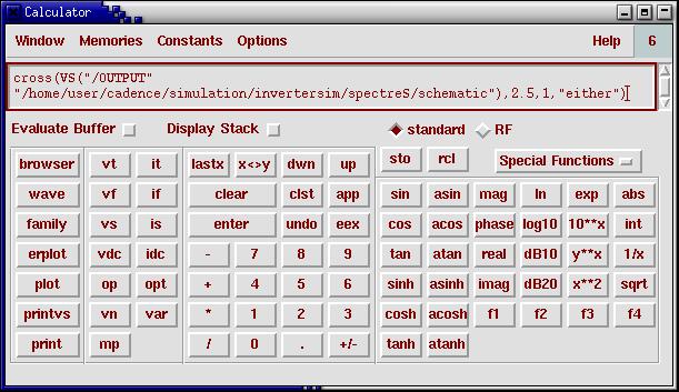
Now that you have completed a transient simulation of the inverter, you want to know the characteristics of the output, such as the rise time, the fall time, and the delay time. All of these characteristics, plus many more, can be calculated using the Waveform Calculator. In the Waveform Window, select the third to last icon that looks like a calculator, labeled "Calculator".

The functions delay() and riseTime() can be use to calculate the delay time, and rise and fall times, respectively. These functions can be selected using the "Special Functions" menu or can be typed in manually. This tutorial will show you how to do it both ways. Knowing how to use the functions manually will enable the user to write the functions in a report without having to use the calculator. Besides what this tutorial teaches you, don't be afraid to explore the calculator more and find out what else it can do.
The riseTime function has 7 input arguments, but you only really need to worry about three of them. The rise time is defined as the time between 10% and 90% of the final value of the rising edge. Fall time is the same thing, but for the falling edge.
riseTime(voltage_waveform start_time t end_time t 10 90)
voltage_waveform - This argument is the actual waveform you want to find the rise time of. Use the VT function to indicate you are looking at the voltage waveform. Example: VT( "/OUTPUT" ) ...where /OUTPUT is the name of the waveform in the Waveform Window.
start_time - This argument can be represented by a number or a marker. A marker is probably easier to use. When calculating the rise time, this argument must occur before the rising of the waveform begins. When calculating the fall time, this argument must occur before the falling of the waveform begins.
end_time - This argument can be represented by a number or a marker. A marker is probably easier to use. When calculating the rise time, this argument must occur after the rising of the waveform begins. When calculating the fall time, this argument must occur after the falling of the waveform begins.
The delay function has 8 input arguments. The user has to indicate the name, voltage threshold, edge, and edge type of each waveform. This function calculates the timing between the voltage threshold of the rising edge of one waveform and the voltage threshold of the falling edge of another waveform. In most cases, the voltage thresholds will be set to 50% of their respective maximum voltage.
delay(voltage_waveform1,voltage_threshold1,edge_number1,"edge_type",voltage_waveform2,voltage_threshold2, edge_number2,"edge_type")
voltage_waveform1/2 - This argument is the actual waveform you want to find the rise time of. Use the VT function to indicate you are looking at the voltage waveform. Example: VT( "/OUTPUT" ) ...where /OUTPUT is the name of the waveform in the Waveform Window.
voltage_threshold1/2 - This argument requires a voltage threshold value to indicate either where the timing starts or ends.
edge_number1/2 - This argument indicates the n-th edge. So, if the argument was 2, then it would find the 2nd edge.
edge_type - This argument indicates the type of edge: rising, falling, or either.
Before calculating these values, let's define 2 vertical markers for the riseTime function. First, go to the Waveform Window and zoom in by typing 'z' and clicking your mouse to outline one of the transition areas of the waveforms (a rising edge of the output). Once you have zoomed in to the desired area, select Markers -> Vertical Marker ...

Once the Vertical Markers window opens, select "Add Graphically" and in the Waveform Window, place the markers before and after the rising of the output begins and ends.

Return to the Calculator window and type the following in the window:
riseTime(VT("/OUTPUT") M1 t M2 t 10 90)
After you have typed this command (without commas between arguments), select the enter button and the command should be replaced with a value. This value is your rise time.


Make sure that "Evaluate Buffer" is not selected. Click on the wave button, and then select the output waveform. Then, in the Calculator window, select "Special Functions" and then "riseTime" from the list. A new window entitled "Rise Time" will appear and you will prompted to enter initial and final values. Verify that the "y to x" buttons are selected, and type M1 and M2, respectively.

Then, select OK and "Evaluate Buffer" in the Calculator window. The results will be displayed in the window.
Ensure that "Evaluate Buffer" is not selected. In the Waveform Window, type "F" to zoom out and fit the waveforms to the window. Place the markers (in the same order) around a falling edge of the output. Zoom in if you need to. Then repeat the steps above either manually or using the calculator buttons.
You do not need to use the markers for calculating the delay. Enter the following command (with arguments having commas between them) in the calculator window
delay(VT("/net2"),2.5,1,"either",VT("/OUTPUT"),2.5, 1,"either")
After selecting the enter button, the screen will tell you your delay time. If
First, ensure that "Evaluate Buffer" is not selected. Then, select the wave button and select the input waveform in the Waveform Window. Then, select "Special Functions" and "delay" from the list. A new window entitled "Threshold Delay" will appear. You can leave the default values. The calculator will have automatically placed the correct arguments in for the input and output waveforms.

Then, select OK and "Evaluate Buffer" in the Calculator Window. The calculator will have automatically placed the correct arguments in for the input and output waveforms. The results will be displayed in the window.
If you would like to test the accuracy of these tools, manually measure the rise, fall, and delay times and see how well they match up. It may be difficult to manually measure a timing as accurate as the functions can compute them though. A good method of calculating these values is using the crosshair markers.
To calculate the rise time of the output, first zoom into a rising edge of the output in the Waveform Window.
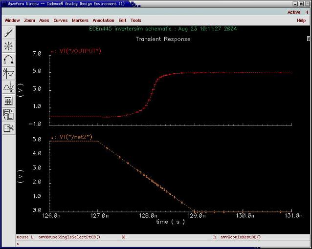
Then, type 'a' for the a-crosshair marker and place it (by viewing the x/y coordinates in the upper-left corner) at y = 0.5 (10% of final value). Then, type 'b' for the b-crosshair marker and place it at y = 4.5 (90% of final value). You may not be able to place the markers at these exact locations.

Notice at the bottom left corner of the Waveform Window, that the crosshair markers have been listed, along with a delta value (x-coordinate of b minus x-coordinate of a).
![]()
Therefore, the rise time (delta value) is approximately 512.719 picoseconds. Remember, the calculator is probably more accurate because it is calculating the rise time between points at 0.5 V and 4.5 V. With the crosshair markers, for this example, the rise time was calculated for points 497.954 mV and 4.50122 V. You might want to try calculating the fall time and delay time using the crosshair markers and then compare these values to the calculator values.
For the DC simulation, we will sweep the input of the inverter, 0 to 5 volts. To do this, first open up the schematic that is set up to simulate the inverter. Then, select Tools -> Analog Environment, to open the Cadence Analog Design Environment window.
Verify that the simulator that you are using is "spectreS". If not, change the simulator to spectreS by selecting Setup -> Simulator/Directory/Host ... Now, select Analyses -> Choose ...
Select the DC box under the analysis list. Also, select "Component Parameter" and "Select Component". In the Virtuoso schematic window, select the voltage source that is connected to the input of the inverter. A list of parameters of the voltage source will appear. Choose "dc" and make sure in the analysis setup window, that the Sweep Range has "Start-Stop" selected and 0 and 5 are in the "Start" and "Stop" parameters, respectively. Also, make sure that the Sweep Type reads "Automatic".

Now, you are ready to simulate. Select the output and input of the inverter to plot and run the simulation. The DC Response should look something like the waveform below.

Notice how the input and output cross in the linear (transition) region of the inverter. We will want to calculate this crossing value so that it can be used as a bias to the input of the inverter for future AC simulation. This can be accomplished either by eyeing it or more effectively by using the calculator.
Open the calculator by selecting the calculator icon. Make sure that "Evaluate Buffer" is unchecked. Select wave, and then click on the output waveform in the Waveform Window. Now, select "Special Functions" and choose "cross" in the Calculator window. When the "Threshold Crossing" window appears, select OK for the default values. Select "Evaulate Buffer" in the Calculator Window, and the cross value will be given. This should be roughly vdd/2 (vdd/2 is for an ideal inverter). Round off to the nearest hundreth and remember this value for AC simulation.


Before doing an AC simulation, a change needs to be made to the schematic that is testing the inverter. The pulse source needs to be changed to a sine wave source. This source can found in the "NCSU_Analog_Parts" library, under the "Voltage_Sources" category. Change the following parameters:
Check and save your schematic and choose Tools -> Analog Environment if you don't already have the Cadence Analog Design Environment window open. Select Analyses -> Choose ... When the Choosing Analyses window opens, select AC analysis. Make sure that "Frequency" is selected and 10 and 1000M are the start and stop frequencies, respectively. Also, select a logarithmic sweep with 10 points per decade. Choose OK.

Next, run the simulation. Select Results -> Direct Plot -> AC Magnitude & Phase in the Cadence Analog Design Environment window to view the frequency response of the AC simulation.
